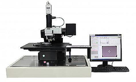
Thickness measurement | 박막 두께 측정기

| Laboratory/Field | |||
|---|---|---|---|
| Model | ST4000-DLX | ||
| Maker | K-MAC | ||
| Technician | Min-jae Kim | ||
| Contact | 052-217-4064 / mjkim@unist.ac.kr | ||
| Status for Reservation | 가능 | ||
| Reservation Unit | 30min | Maximum Time (per day) | 1hr |
| Open(~ago) | 2주전 | Cancel (~ago) | 2hr |
| Equipment location | 108동 B101호 (Bldg. 108, Room B101) | ||
-
Description
Some portion of the light that is incident on the thin film surface is reflected
from the upper surface of the sample, other portion is reflected from the
interfaces between the thin film and the substrate. -
Specifications
• Detector : used wavelength range is 400 ~ 800 nm
linear silicon CCD array (2048 pixel)
• Stage size : 300 mm x 300 mm (12 inch wafer)
• Lens : m 5 x, m10 x, m 50 x
• Spot size : 40μm, 20μm, 4μm
• Reflection probe : choose wavelength (300 ~ 800 nm)
• Thickness measurement range : 100 Å ~ 50μm
• Theoretical resolution : 1 nm
-
Applications
• Semiconductor : Poly-Si, GaAs, GaN, ZnS, SiGe, ONO, SOI, SiLk
• Dielectric material : SiO2, Si3N4, ITO, TiO2, ZrO2, BTS, HfO2
• Polymer : PVA, PET, PP, PR