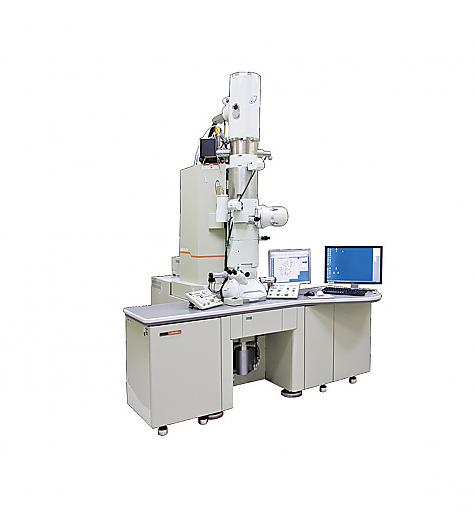
JEM-2100F(투과전자현미경5, HR-TEM) | 투과전자현미경5
| Laboratory/Field | |||
|---|---|---|---|
| Model | JEM-2100F | ||
| Maker | JEOL | ||
| Technician | Jeong-hwan Lim | ||
| Contact | 052-217-4175 / jhwan0918@unist.ac.kr | ||
| Status for Reservation | 불가능 | ||
| Reservation Unit | 0.5hr | Maximum Time (per day) | 2hr |
| Open(~ago) | 5일전 | Cancel (~ago) | 2시간전 |
-
Description
TEM is used to analyze micro-structures of materials with high spatial resolution. The high voltage electron beam generated from electron gun is illuminated on thin film specimen. The beam penetrating the specimen passes through an array of magnetic lenses and forms a high resolution electron image of the electron diffraction pattern.
-
Specifications
• Acceleration voltage : 200 kV
• Lattice resolution : 0.102 nm
• BF-STEM resolution : 0.14 nm (Gatan)
• HAADF-STEM resolution : 0.096 nm (Jeol)
• Probe stability : 1 nm/min or less
• Stage stability : 1 nm/min or less
• EDS resolution : 128 eV (Oxford, x-Max T-80)
• EELS resolution : 0.8 eV (Gatan, Enfina)
• Contamination : 1 nm/min or less
-
Applications
• Ultra high resolution electron imaging
• Diffraction pattern
• STEM imaging (BF, HAADF)
• Energy dispersive spectroscopy (EDS)