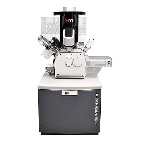
Helios 450HP FIB | 이온집속빔

| Laboratory/Field | |||
|---|---|---|---|
| Model | Helios NanoLab 450 | ||
| Maker | FEI | ||
| Technician | Sun-yi Lee | ||
| Contact | 052-217-4023 / ssun295@unist.ac.kr | ||
| Status for Reservation | 가능 | ||
| Reservation Unit | 0.5hr | Maximum Time (per day) | 4hr |
| Open(~ago) | 5일전 | Cancel (~ago) | 2시간전 |
| Equipment location | 102동 B108호 | ||
-
Description
샘플 배송 주소
울산시 울주군 언양읍 유니스트길 50, 102동 201-5호Dual-beam FIB has a multitude of capabilities including high resolution electron imaging, ion imaging, nano device fabrication, and material deposition. Simultaneous patterning and imaging are possible to nm resolution for both imaging and machining. FIB with both ion and electron beams enables highprecision cross-section processing and TEM/3DAP sample preparation.
-
Specifications
• Electron optics - Resolution
HV : 0.9 nm @15 kV, 1.4 nm @1 kV
- Accelerating voltage : 1 kV ~ 30 kV
- Probe current : up to 200 nA
- Magnification : 30 x ~ 1,280 kx
• Ion optics - Resolution : 5 nm @30 kV
- Beam voltage : 500 V - 30 kV
• Multi chem gas injection systems (C, Pt, W, H2O)
-
Applications
• Ultra high resolution electron, ion imaging
• TEM sample preparation
• Energy dispersive spectroscopy (EDS)
• SE, BSE imaging