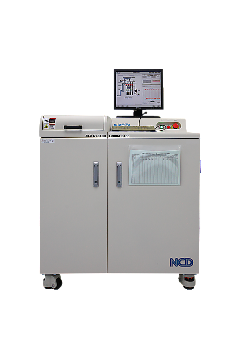
Atomic Layer Deposition | 원자층 증착 장비

| Laboratory/Field | |||
|---|---|---|---|
| Model | Lucida D100 | ||
| Maker | NCD | ||
| Technician | Kim Boseong | ||
| Contact | 052-217-4191 / mbosing@unist.ac.kr | ||
| Status for Reservation | 가능 | ||
| Reservation Unit | 3hr | Maximum Time (per day) | 5hr |
| Open(~ago) | 2주전 | Cancel (~ago) | 2hr |
| Equipment location | 108동 B101호 (Bldg. 108, Room B101) | ||
-
Description
ALD is a thin film deposition technique that is based on the sequential use of a gas phase chemical process. The majority of ALD reactions use two chemicals, typically called precursors. These precursors react with the surface of a material one at a time in a sequential, self-limiting, manner. Through the repeated exposure to separate precursors, a thin film is slowly deposited.
-
Specifications
• Substrate size : 4 ~ 8 inch silicon wafer
• Substrate temperature
- 25 °C ~ 350 °C (± 0.2 °C) @1 Torr, in wafer
• Deposition uniformity : less than ± 2 % within wafer
• Precursor sources
- 3, heated 2 sources and H2O source •Substrate size : 4 ~ 8 inch silicon wafer
• Process temperature : 30 °C ~ 450 °C
• Deposition uniformity : less than ± 2 % within wafer
• Dual process mode : termal and plasma
• Shower head type multi-chamber cluster tool
-
Applications
• High-k thin film (HfO2, TiO2, Al2O3) Depo.
• Applications of R&D
• Dielectric thin films : Al2O3, HfO2, etc
• Nitride & metal thin films : TaN, etc