Titan G2(투과전자현미경4_Advanced TEM) | 수차보정 고분해능 투과전자현미경
| Laboratory/Field | |||
|---|---|---|---|
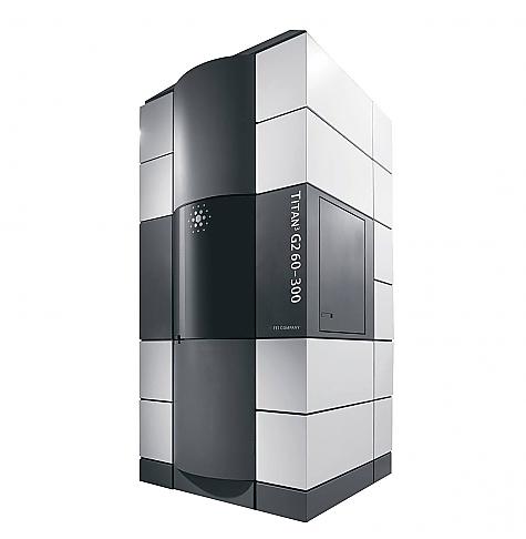
| Model | Titan G2(60-300) | ||
| Maker | FEI | ||
| Technician | Jong Hoon Lee | ||
| Contact | 052-217-4171 / jonghoon@unist.ac.kr | ||
| Status for Reservation | 가능 | ||
| Reservation Unit | 0.5hr | Maximum Time (per day) | 12hr |
| Open(~ago) | 5일전 | Cancel (~ago) | 2시간전 |
| Equipment location | 102동 B112호 (Bldg.102, Room B112) | ||
-
Description
TEM is used to analyze micro-structures of materials with high spatial resolution. The high voltage electron beam generated from electron gun is illuminated on thin film specimen. The beam penetrating the specimen passes through an array of magnetic lenses and forms a high resolution electron image of the electron diffraction pattern.
-
Specifications
• Acceleration voltage : 60 - 300 kV
• Lattice resolution : 0.065 nm
• BF-STEM resolution : 0.14 nm
• HAADF-STEM resolution : 0.12 nm
• Probe stability : 1 nm/min or less
• Stage stability : 1 nm/min or less
• EDS resolution : 128 eV
• EELS resolution : 0.16 eV
• Contamination : 1 nm/min or less
-
Applications
• Sub angstrom spatial resolution TEM
• Atomic resolution at low kV
• Imaging and spectroscopy of soft matters
• Dynamics of individual atoms
• High energy resolution EELS and EDS
• Energy-filtered imaging and diffraction