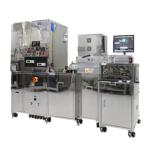
PE CVD_#3 (TTL) | 플라즈마 화학기상 증착기 Ⅲ
| 연구실/분야 | |||
|---|---|---|---|
| 모델명 | FABStar+ | ||
| 제조사 | TTL | ||
| 담당자 | 강해라 | ||
| 연락처 | 052-217-4167 / haera@unist.ac.kr | ||
| 예약 가능여부 | 가능 | ||
| 예약단위 | 2hr | 1일최대예약시간 | 3hr |
| 예약Open(~일 전) | 2주전 | 예약취소불가(~일 전) | 1hr |
| 장비위치 | 108동 B101호 (Bldg. 108, Room B101) | ||
-
Description
PECVD System is capable of deposition silicon nitride and silicon carbide using electron energy (plasma) as the activation method to enable deposition at a low temperature and at a reasonable rate.
-
Specifications
• Wafer Size : piece ~ 6 inch silicon wafer
Substrate temperature : ~ 350 °C
• High plasma density, high dep. rate PE-CVD
• Process gas : N2, He, SF6 /O2, pure SiH4 /NH3 /CH4
• Power supply : 600 W, 13.56 MHz RF Generator
• Process guarantee : 1000 Å ~ 1 um
• Uniformity : less than ± 3 % within wafer
• Uniform process gas flow distribution
-
Applications
• High rate and high quality silicon carbide deposition with stress control
• Passivation layer
• Inter metal dielectric of semiconductor
• Inter layer dielectric of semiconductor