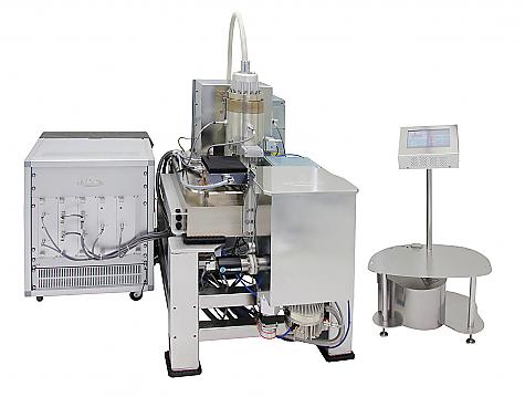
E-beam lithography | 전자선 노광장치 시스템
| 연구실/분야 | |||
|---|---|---|---|
| 모델명 | NB3 | ||
| 제조사 | NBL | ||
| 담당자 | 이루다 | ||
| 연락처 | 052-217-4022 / [email protected] | ||
| 예약 가능여부 | 가능 | ||
| 예약단위 | 4hr | 1일최대예약시간 | 24hr |
| 예약Open(~일 전) | 2주전 | 예약취소불가(~일 전) | 24hr |
| 장비위치 | 108동 B101호 (Bldg. 108, Room B101) | ||
-
Description
As the primary electron beam penetrates the resist, elastic collisions spread the beam slightly. Backscattered electrons from the substrate may be spread over several microns. The secondary electrons generated in this process impart energy to resist through inelastic collisions. This causes the physical and chemical changes in the resist that renders in more soluble than the unexposed resist.
-
Specifications
• Theoretical beam size : 2.1 nm @100 keV, 7 nA
• Line width : < 5 nm
• Deflection : vector scan, 55 MHz
• Address grid resolution : 1 nm, 1 mm main field
• Beam voltage : 30 ~ 100 keV
• Writing area : 195 mm × 195 mm
• Repeatable : 20 nm over wafer
-
Applications
• nm level device fabrication
• Generating fine patterns
• Mask manufacture
• Optical device fabrication
• Contacts for Nanowires/rods