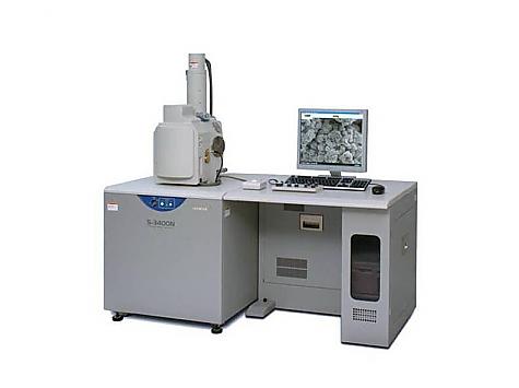
S-3400N Scanning Electron Microscope | 전자현미경

| Laboratory/Field | |||
|---|---|---|---|
| Model | S-3400N(Type Ⅱ) | ||
| Maker | Hitach High-Technologies | ||
| Technician | Min-jae Kim | ||
| Contact | 052-217-4064 / mjkim@unist.ac.kr | ||
| Status for Reservation | 가능 | ||
| Reservation Unit | 1hr | Maximum Time (per day) | 1hr |
| Open(~ago) | 2주전 | Cancel (~ago) | 2hr |
| Equipment location | 108동 B101호 (Bldg. 108, Room B101) | ||
-
Description
SEM is a microscope that uses electrons instead of light to form an image. The scanning electron microscope has many advantages over traditional microscopes.
-
Specifications
• Magnification : x 5 to x 300,000 (continuous)
• Accelerate voltage : 0.3 to 30 kV (0.1 kV/step)
• Detector : SE+BSE
• Electrical image shift : ± 50μm (WD = 10 mm)
• Electron gun : precentered cartridge filament
• Traverse : X axis 0 ~ 100 mm, Y axis 0 ~ 50 mm
-
Applications
• Microstructure analysis of the sample, such as a wide range of metal, materials, semiconductors, fiber and polymer material.
• Surface microstructure of the metal, the material and shape of analysis.