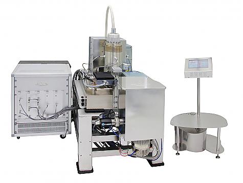
E-beam lithography | 전자선 노광장치 시스템
| Laboratory/Field | |||
|---|---|---|---|
| Model | NB3 | ||
| Maker | NBL | ||
| Technician | Luda Lee | ||
| Contact | 052-217-4022 / luda30159@unist.ac.kr | ||
| Status for Reservation | 가능 | ||
| Reservation Unit | 4hr | Maximum Time (per day) | 24hr |
| Open(~ago) | 2주전 | Cancel (~ago) | 24hr |
| Equipment location | 108동 B101호 (Bldg. 108, Room B101) | ||
-
Description
As the primary electron beam penetrates the resist, elastic collisions spread the beam slightly. Backscattered electrons from the substrate may be spread over several microns. The secondary electrons generated in this process impart energy to resist through inelastic collisions. This causes the physical and chemical changes in the resist that renders in more soluble than the unexposed resist.
-
Specifications
• Theoretical beam size : 2.1 nm @100 keV, 7 nA
• Line width : < 5 nm
• Deflection : vector scan, 55 MHz
• Address grid resolution : 1 nm, 1 mm main field
• Beam voltage : 30 ~ 100 keV
• Writing area : 195 mm × 195 mm
• Repeatable : 20 nm over wafer
-
Applications
• nm level device fabrication
• Generating fine patterns
• Mask manufacture
• Optical device fabrication
• Contacts for Nanowires/rods